
Intel | Intel 8008 CPU | Microprocessor
In the ever-evolving landscape of computer technology, certain milestones stand out as transformative moments that shape the course of history. One such landmark achievement was the birth of the Intel 8008 microprocessor. Released in April 1972, this groundbreaking 8-bit CPU, with its external 14-bit address bus, laid the foundation for the future of computing. Initially known as the 1201 and commissioned by Computer Terminal Corporation (CTC), the Intel 8008 encountered a twist of fate that led to its unexpected journey beyond its original intended purpose.
Designed to implement CTC’s instruction set for their Datapoint 2200 programmable terminal, the Intel 8008 faced challenges and delays during its development, ultimately resulting in CTC opting to use its own TTL-based CPU instead. Seizing the opportunity, Intel secured an agreement to market the 8008 to other customers. It was Seiko, the renowned Japanese manufacturer of calculators, who expressed interest in utilizing this revolutionary chip for their calculator designs.
In this article, we delve into the fascinating origins, features, and impact of the Intel 8008 microprocessor. By examining its early days as the 1201 and tracing its unexpected divergence from CTC’s initial plans, we uncover the crucial role it played in the birth of the microprocessor revolution. Join us on a journey to unravel the legacy of the Intel 8008 and its pivotal contribution to shaping the landscape of modern computing as we know it today.
History
The history of the Intel 8008 processor is a tale of innovation, challenges, and the birth of a groundbreaking technology that would shape the future of computing. It all started in 1968 when Computer Terminal Corporation (CTC) was established under the guidance of Austin O. “Gus” Roche and Phil Ray, both NASA engineers with a passion for cutting-edge technology.
CTC’s original plan was to create a desktop computer, but the market was not yet ready for such a revolutionary concept. Instead, they focused on developing a Teletype Model 33 ASR replacement, which eventually became the Datapoint 3300. This innovative machine, designed to fit the same space as an IBM Selectric typewriter, featured a video screen with the aspect ratio of an IBM punched card. Although successful, the compact design of the Datapoint 3300 led to ongoing heat problems due to the densely packed circuitry.
To overcome these challenges and improve the system, CTC embarked on a redesign that involved implementing the central processing unit (CPU) portion of the internal circuitry on a single chip. Seeking a company capable of producing their chip design, Gus Roche approached Intel, primarily known as a supplier of memory chips at the time. However, Intel’s co-founder, Bob Noyce, had reservations about the concept. He believed that selling computer chips would limit their market to just one chip per computer, unlike memory chips that could be sold in larger quantities.
Despite the concerns, Noyce agreed to a $50,000 development contract in early 1970, signaling Intel’s entry into the processor market. Texas Instruments (TI) also joined as a secondary supplier. However, the initial chip samples produced by TI based on Intel’s drawings proved to be buggy and were rejected. Intel’s own versions faced delays, prompting CTC to pursue an alternative approach. They decided to redesign their terminal using discrete transistor-transistor logic (TTL) instead of waiting for a single-chip CPU.
The result was the release of the Datapoint 2200 in the spring of 1970, which marked their first sale to General Mills on May 25, 1970. Meanwhile, six months later, Seiko, inspired by the success of Intel’s simpler 4004 chip, approached Intel expressing interest in using their new processor, now known as 1201, in a scientific calculator. Under the leadership of Federico Faggin, the designer of the 4004, a small redesign was undertaken, and 1201 was delivered to CTC in late 1971.
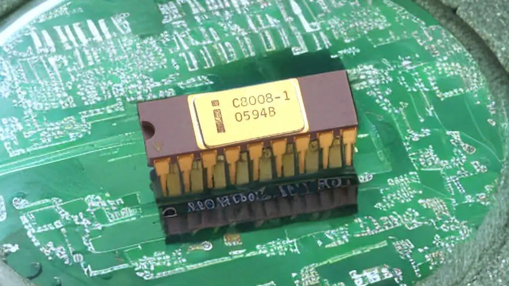
However, CTC had already moved on to the more advanced Datapoint 2200 II, rendering 1201 insufficient for their new model. As a result, CTC made the strategic decision to discontinue its engagement with the 1201 chip, opting to forgo its contractual obligation of paying $50,000 to Intel and relinquishing its intellectual property rights to the processor instead. Intel rebranded the chip as the Intel 8008 and introduced it in their catalog in April 1972, pricing it at $120. This name change aimed to capitalize on the success of the 4004 chip, even though the 8008 was a distinct design from its predecessor.
The Intel 8008 processor quickly gained traction in the market, establishing itself as the CPU of choice for the earliest commercial non-calculator personal computers. This included notable systems like the US SCELBI kit and the French Micral N. These pioneering machines, driven by the power of the Intel 8008, ushered in a new era of personal computing, transforming the way individuals engaged with technology and setting the stage for future innovations in the field. It also served as the controlling microprocessor for several models of Hewlett-Packard’s computer terminals.
The journey of the Intel 8008 was just the beginning. It paved the way for the subsequent development of the Intel 8080 and the immensely successful Intel x86 family, leaving an indelible mark on the history of computing. The Intel 8008, with its innovative architecture and pioneering spirit, set the stage for a new era of technological advancements that continue to shape our world today.
Design of Intel 8008 Processor
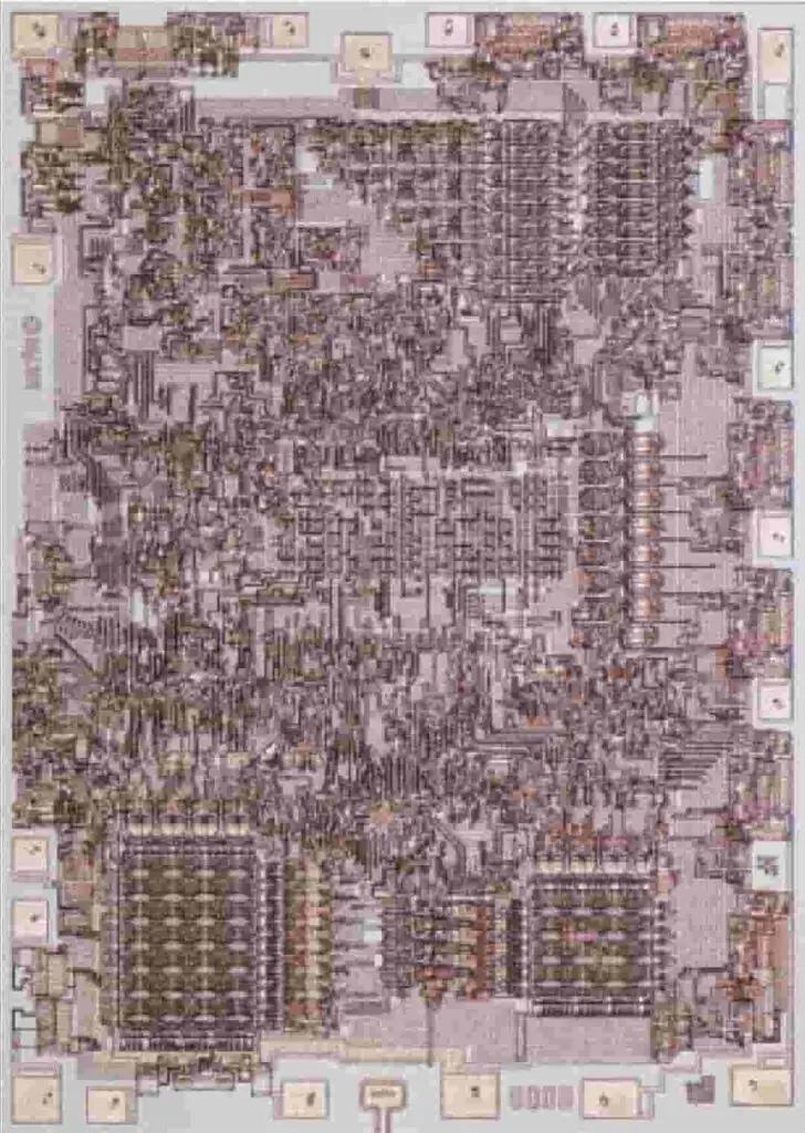
The Intel 8008 processor was a remarkable milestone in the world of microprocessor design. Developed using 10 μm silicon-gate enhancement-mode PMOS logic, it represented a significant leap forward in technological advancement. The processor was initially capable of operating at clock frequencies of up to 0.5 MHz, which was later improved to a maximum of 0.8 MHz in the upgraded 8008-1 version.
- Initial clock speed: 800 kHz
- Transistors: 3,500
- Manufacturing technology: 10 microns.
Instructions in the Intel 8008 were executed using a T-state model, where each T-state consisted of two clock cycles. The number of T-states required for instruction completion varied, ranging from 5 to 11. Register-to-register loads and arithmetic logic unit (ALU) operations took 5 T-states (equivalent to 20 microseconds at 0.5 MHz), register-to-memory operations required 8 T-states (32 microseconds), and calls and jumps, when taken, consumed 11 T-states (44 microseconds).
While the Intel 8008 may have had a slightly slower instructions-per-second rate compared to the 4-bit Intel 4004 and Intel 4040 processors, it offered a distinct advantage by processing data in 8-bit units. Additionally, its ability to access a larger amount of random access memory (RAM) granted it a significant speed advantage in most applications. With a transistor count of 3,500, the Intel 8008 pushed the boundaries of what was achievable during that early era of microprocessors.
The design of the Intel 8008 featured a single 8-bit bus and required external support logic due to its 18-pin dual in-line package (DIP) configuration. For memory access, the 14-bit address required additional logic to be latched into an external memory address register (MAR). The processor also boasted 8 input ports and 24 output ports, making it particularly suitable for controller and cathode ray tube (CRT) terminal applications. However, compared to subsequent generations of microprocessors, the Intel 8008’s design proved somewhat cumbersome for other tasks.
While a handful of early computer designs were based on the Intel 8008, the majority of systems favored the enhanced capabilities of the Intel 8080 processor, which surpassed its predecessor in terms of performance and features.
Features of Intel 8008 Processor
The Intel 8008 processor, renowned for its pioneering role in the microprocessor revolution, boasted a range of impressive features that set it apart. Let’s explore some of the key features that made the 8008 architecture a game-changer.
At the heart of the 8008 lay seven “scratchpad” registers, each capable of holding 8 bits of information. These registers included the main accumulator (A) and six additional registers (B, C, D, E, H, and L). They acted as temporary storage areas where data could be manipulated and processed, enabling the processor to perform various operations with efficiency.
Another essential element of the 8008’s architecture was its 14-bit program counter (PC). The program counter kept track of the memory location of the next instruction to be executed, ensuring the seamless flow of program execution. This feature allowed the processor to follow a predetermined sequence of instructions, executing commands in the desired order.
The Intel 8008 also introduced a seven-level push-down address call stack, an innovative mechanism for managing program flow. The call stack utilized eight registers, with the topmost register dedicated to storing the program counter (PC). This stack-based approach facilitated efficient subroutine calls and returns, enabling the processor to handle complex tasks and efficiently manage program execution.
To keep track of various conditions during program execution, the 8008 incorporated four condition code status flags. These flags included carry (C), even parity (P), zero (Z), and sign (S). By monitoring these flags, the processor could make decisions based on the outcomes of specific operations, allowing for more sophisticated program control and error handling.
One of the notable capabilities of the Intel 8008 was its support for indirect memory access. This was achieved through the use of the H and L registers, which, when combined with the HL register, formed a 14-bit data pointer. Although the upper two bits of the HL register were ignored, the remaining 14 bits allowed for indirect memory addressing. This feature enabled the processor to access data stored in memory through a flexible and efficient mechanism.
In summary, the Intel 8008 processor revolutionized the world of microprocessors with its impressive set of features. The scratchpad registers, program counter, call stack, condition code flags, and indirect memory access capabilities all contributed to the processor’s ability to execute complex instructions, handle data efficiently, and provide flexible program control. These features laid the groundwork for the evolution of microprocessors and set the stage for the remarkable advancements that followed in the world of computing.
Also Read: Timeline and Generations of Intel Processors | Advancement of Intel Processors
FAQ
What is the Intel 8008 microprocessor?
The Intel 8008 microprocessor is an 8-bit CPU that played a pivotal role in the history of computing. It was originally known as the 1201 and was designed for the Datapoint 2200 terminal but ended up being marketed by Intel for other applications.
What was the significance of the Intel 8008?
The Intel 8008 was a landmark achievement in microprocessor technology. It was one of the earliest microprocessors and laid the foundation for future advancements in computing. Its architecture and features set the stage for the microprocessor revolution that followed.
How did the Intel 8008 come into existence?
The Intel 8008 originated from a development contract between Computer Terminal Corporation (CTC) and Intel. CTC initially planned to use the 8008, then known as the 1201, in their Datapoint 2200 terminal but opted for a different approach due to delays. Intel rebranded the chip and introduced it to the market independently.
What were the features of the Intel 8008 microprocessor?
The Intel 8008 had several notable features, including seven scratchpad registers for temporary storage, a 14-bit program counter for instruction sequencing, a seven-level call stack for efficient subroutine handling, condition code status flags for decision-making, and support for indirect memory access.
How did the Intel 8008 impact the computing landscape?
The Intel 8008 was a game-changer in the world of microprocessors. It was used in early non-calculator personal computers and computer terminals, paving the way for the development of subsequent processors like the Intel 8080 and the popular Intel x86 family. Its influence can be seen in the transformative advancements in computing technology that followed.
What were the limitations of the Intel 8008?
The Intel 8008 had a relatively slow clock frequency compared to later processors, and its external support logic made its design somewhat cumbersome for certain tasks. These limitations prompted the preference for the enhanced capabilities of the Intel 8080 in many systems.
How did the Intel 8008 contribute to the birth of the microprocessor revolution?
The Intel 8008 was a pioneering microprocessor that demonstrated the feasibility and potential of integrating complex computing functions onto a single chip. Its success and impact on early computer systems laid the groundwork for further advancements in microprocessor technology and shaped the direction of computing history.
What other processors followed the Intel 8008?
The Intel 8080 processor succeeded the Intel 8008 and offered improved performance and features. It was followed by the immensely successful Intel x86 family, which became the dominant architecture in the personal computer market and continues to be used today.
What was the price of the Intel 8008 when it was introduced?
The Intel 8008 was introduced at a price of $120.
-
Unveiling the Intel 8008: Pioneering the Era of Microprocessors
Intel | Intel 8008 CPU | Microprocessor In the ever-evolving landscape of computer technology, certain milestones stand out as transformative moments that shape the course of history. One such landmark achievement was the birth of the Intel 8008 microprocessor. Released in April 1972, this groundbreaking 8-bit CPU, with its external 14-bit address bus, laid the…
